High Data-rate Bi-directional CMOS Power/Data Link For Implanted Medical Devices
Background
Implanted medical devices (IMDs) employing bio-signal recording and transcutaneous transmission require a high data rate for the uplink while also being powered wirelessly e.g., intracranial multi-channel ECoG recording. Load Shift Keying (LSK), a widely used modulation scheme for uplink data telemetry, trades off power transfer and data-rate based on the inductive coil’s quality factor Q. High power transfer efficiency requires high Q, normally restricting the data rate. Data rates of 100-500 kbps with simultaneous power transfer have been achieved by LSK, and a few Mbps using multiple dedicated inductive links for data transfer and power transfer have also been realized. Further, using transient response from phase shifts by shorting the secondary LC tank for a half cycle achieves near 1-Mbps data rate with power transfer over single inductive link. However, this scheme loses energy whenever shorting the LC tank because of the subsequent reversal of LC resonance and the recovery time after transmitting one bit limits the data rate. Approaches using higher RF bands require additional complexity in circuits and antenna structures.
Technology Description
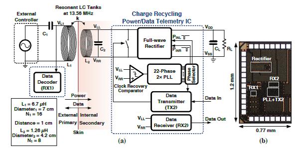
Presented here is a power/data telemetry IC with a new data modulation scheme and simultaneous power transfer through a single inductive link. Data-driven synchronized single-cycle shorting of the secondary LC tank conserves reactive power while inducing an instantaneous voltage change at the primary side. Cyclic on-off keying time-encoded symbol mapping of the shorting cycle allows transmission of two data bits per four carrier cycles with simultaneous power transfer during non-shorting cycles. All timing control signals for rectification and data transmission are generated from a low-power clock recovery comparator and 22-phase 2x PLL.
The 1-mm2 65-nm CMOS IC delivers up to 6.3-mW power and transmits 6.78-Mbps data with a BER of less than 5.9×10⁻⁷ over a single 1-cm 13.56-MHz inductive link.
Figure (a) System Diagram Figure (b) Chip micrograph
Patent Status
| Country | Type | Number | Dated | Case |
| United States Of America | Issued Patent | 9,872,089 | 01/16/2018 | 2014-331 |
Contact
- University of California, San Diego Office of Innovation and Commercialization
- innovation@ucsd.edu
- tel: View Phone Number.

Other Information
Keywords
medical device, implant, wireless